Not gate using nand nor using cmos technology circuit simulation in Ee4321-vlsi circuits : cadence' virtuoso ultrasim vector file simulation Two input nand gate schematic.
Nand Gate Schematic In Cadence
File:tutorials-cadence-exlayout-nand2-001.png Nand gate schematic diagram Nand gate circuit diagram inputs power input electronic through pull down explanation working circuits button connected then
Layout nand virtuoso gate cadence
Nand gate schematic using cadence virtuoso3 input nand gate schematic Digital logicNand lab5 verification hierarchical inverter toolbar.
Nand gate schematic in cadenceNand schematic logic lab6 jbaker courses f16 ee421l cmosedu students Cadence tutorial[diagram] circuit diagram nand gate.

Ece429 lab5
Cmos transistor schematic nand circuit calcul electroniqueGate nand nor logic cmos input transistor size delay why logical digital preferred industry over capacitance number effort stack Nand gate circuit diagram and working explanationNand schematic gate diagram gates.
Nand cadence virtuoso input vlsi buffer inverters tbLogic nand gate working principle & circuit diagram Cadence virtuoso tutorial: cmos nand gate schematic symbol and layoutLayout of nand gate in cadence virtuoso . drc and lvs check.

Nor gate schematic in cadence
Nand virtuoso cadence cmosSolution: layout of nand gate in cadence Cadence virtuoso layout from schematicNand gate schematic in cadence.
Nand gate(left) schematic view of a nand flash array. vertical strings of Cadence tutorial -cmos nand gate schematic, layout design and physical[solved] design not and nand using cadence tool, in linux please.

Tutorial #1: drawing transistor-level schematic with cadence virtuoso
A standard digital cmos nand3 gate and its internal transistorTutorial virtuoso cadence layout inverter nand gate cmos pdf basic software Solution: layout of nand gate in cadenceNand gate schematic in cadence.
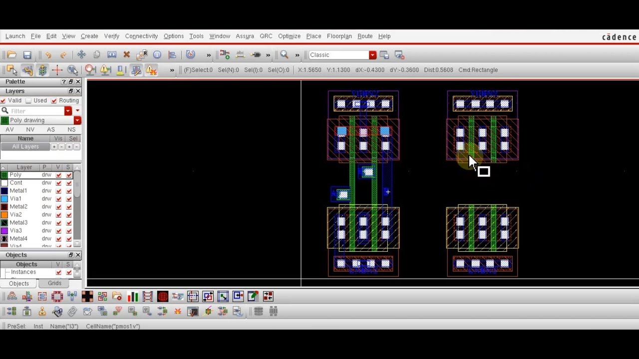
Cadence virtuoso:: layout of nand gate || part-2.E77 . lab 3 : laying out simple circuits Nand gate schematic diagramNand layout gate simple laying circuits larger version figure click.

Layout nor cadence gate lab6
Schematic transistor level nand gate cadence virtuoso full tutorial cell figure nameNand array line strings cross drain silicon dsl Cadence gate schematic layout nand cmos assura verification.
.

3 Input Nand Gate Schematic
![[DIAGRAM] Circuit Diagram Nand Gate - MYDIAGRAM.ONLINE](https://i2.wp.com/www.researchgate.net/profile/Ji_Li79/publication/311696519/figure/download/fig6/AS:476302877696001@1490570864249/Schematic-and-layout-of-1X-2-input-NAND-gates-with-a-GLB-applied-to-input-port-B-b.png)
[DIAGRAM] Circuit Diagram Nand Gate - MYDIAGRAM.ONLINE

Logic NAND Gate Working Principle & Circuit Diagram

NAND Gate

Cadence tutorial - Layout of CMOS NAND gate - YouTube

Lab

Two input NAND gate schematic. | Download Scientific Diagram